Ambient
KP Technology offer a range of Kelvin Probes that work in an ambient environment.
Each system boasting the unique Baikie System to ensure reliable and repeatable measurements to support your research.
Ambient Pressure Photoemission Spectroscopy
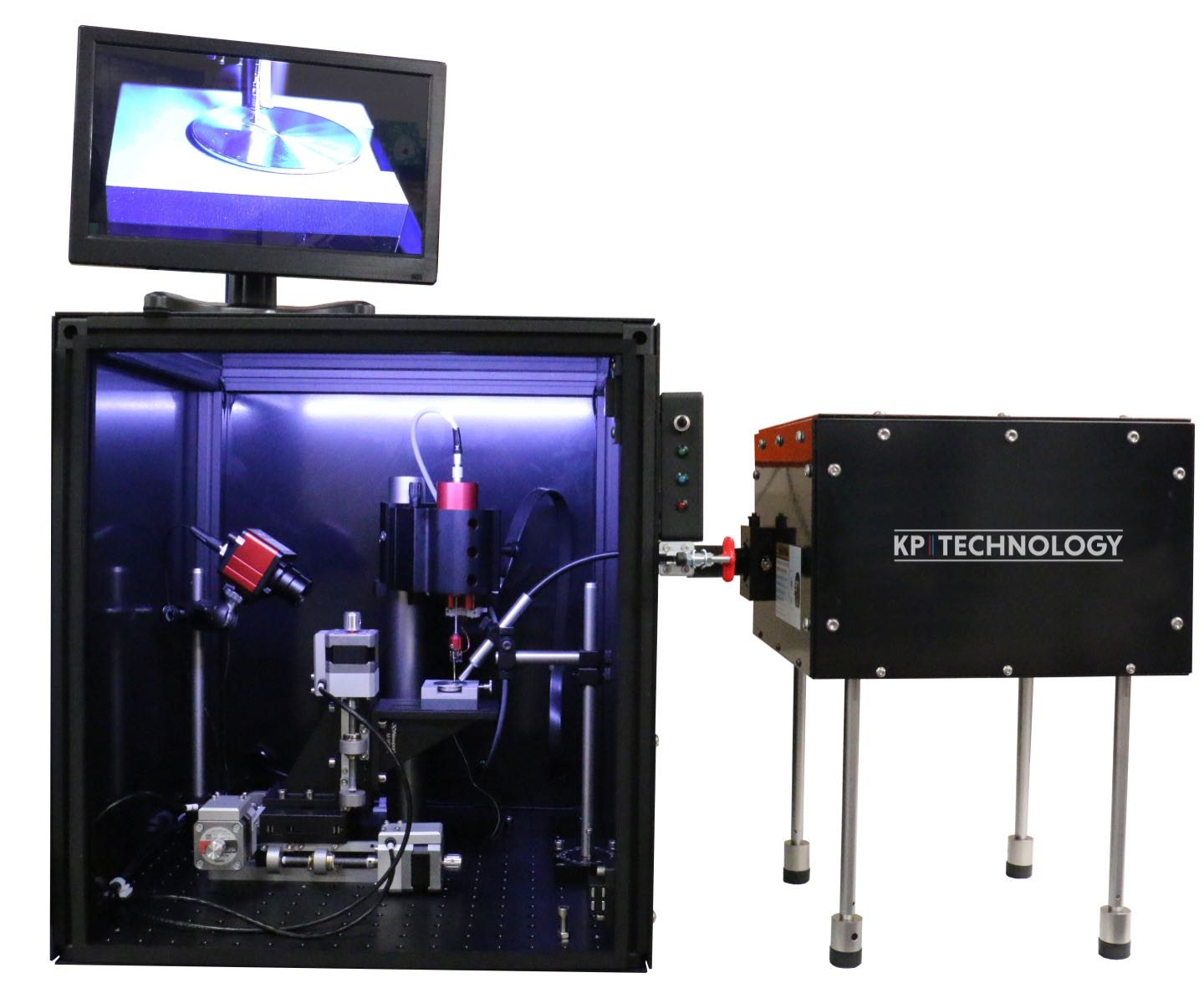
The Ambient Pressure Photoemission Spectroscopy (APS) systems are KP Technology's newest addition to our large surface analysis range. The dual-mode APS systems measure the absolute work function of a material by photoemission in air, no vacuum is required. These systems hold domestic and international patents.
With an excitation range of 3.4 eV to 7.0 eV, the APS systems can measure the absolute work function of metals (accuracy: 0.05 eV) and the ionisation potential of semiconductors alongside measurement of the surface Fermi level with the Kelvin Probe (accuracy: 0.001 eV).
With the addition of a surface photovoltage (SPV) and surface photovoltage spectroscopy (SPS), the full bands of semiconductors can be measured in one system; no other product can do this.
The latest materials and applications highlighted in published papers includes, Perovskite solar cells, indium zinc tin oxide thin films, diamond electronics, organic solar cells, light-emitting electrochemical cells, organic transistors, alkali oxide thin films and semiconductors.
Download the product brochure for more information on the Ambient Pressure Photoemission Spectroscopy range, including technical specifications, example measurements and add-on options.
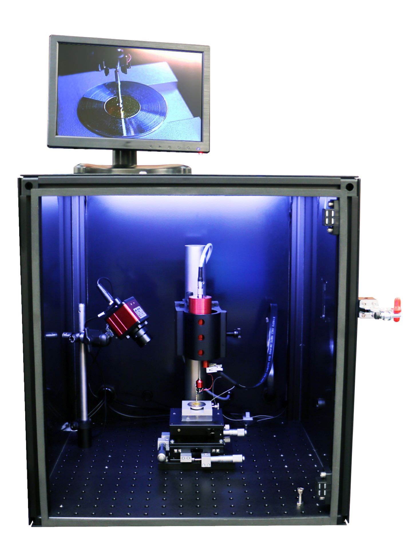
Scanning Kelvin Probe
Our large range of Scanning Kelvin Probes gives the user full access to 2D and 3D work function plots of samples ranging in size from 50 mm to 350 mm. With work function resolution of 1 - 3 meV, and the spatial resolution of the Probe tip diameter (0.05 mm with the SKP5050 model), the Scanning Kelvin Probe gives reliable, repeatable measurements for work function, contact potential difference and Volta potential.
A high performance optical/Faraday enclosure shields all our scanning systems from unwanted fast changing environmental conditions, electromagnetic interference and provides the perfect platform for our Ambient Pressure Photoemission Spectroscopy and Surface Photovoltage add-on modules.
The latest materials and applications highlighted in published papers includes, corrosion protection, carbon steel, thin films, solar cells, molybdenum oxide, zinc oxide nanowire films, quantum dots, hole-transport, nanoparticles, graphene and organic light emitting diodes.
Download the product brochure for more information on the Scanning Kelvin Probe range, including technical specifications, example measurements and add-on options.
Single Point Kelvin Probe
Our Single-Point Kelvin Probe system (KP020) is the introductory system in the KP Technology product family. The off-null signal detection method allows high-quality measurements of the Work Function/Fermi Level of materials.
This entry level, economic system enables users to quickly record non-scanning data and the dedicated software allows full digital control of all parameters to match the exact requirements of the sample under investigation. The recorded data is easily exportable to analysis software.
For rapid events, the KP020 can record work function at a rate of over 300 work function measurements per minute, or, alternatively, the system will track slow work function evolution over several days.
There is an in-built height regulation feature to control the tip to sample spacing during measurements which allows stable, reliable, and repeatable data.
The latest materials and applications highlighted in published papers includes, Perovskite solar cells, molybdenum disulfide, organic photovoltaics, n-type doping, hole-transport, OLEDs, transistors, copper oxide thin films, graphene, quantum dots and solar cells.
Download the product brochure for more information on the KP020, including technical specifications, example measurements and add-on options.
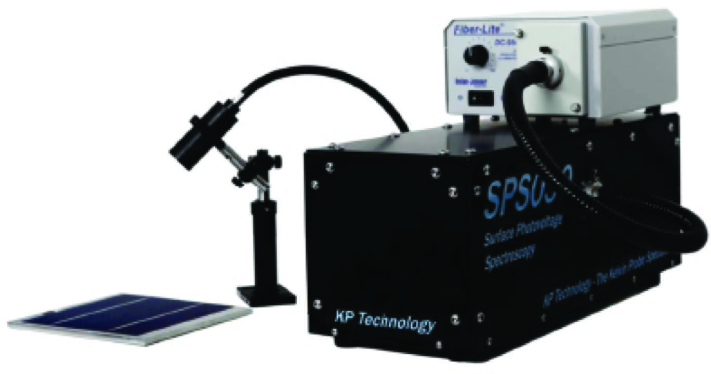
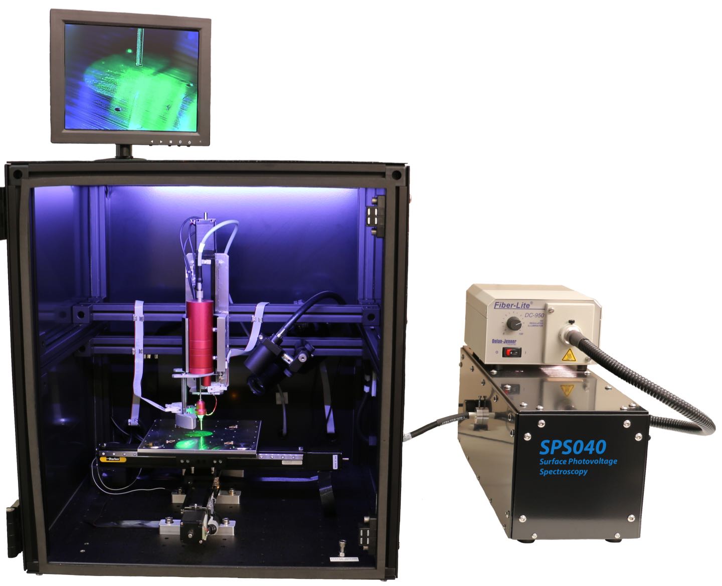
Surface Photovoltage
The surface photovoltage spectroscopy modules are the perfect all-in-one solution for in-depth studies of light sensitive materials such as organic semiconductors, solar cells or light sensitive dyes.
The modules offer a comprehensive range of measurement modes including DC and AC surface photovoltage studies utilising the built-in optical chopper.
Total digital control of all parameters including light intensity and wavelength (400 - 700 nm: SPS030 or 400 - 1000 nm: SPS040) gives the opportunity to investigate and characterise the surface photovoltage and surface photovoltage spectroscopy properties of samples.
The latest materials and applications highlighted in published papers includes, gold films, perovskite solar cells, titanium dioxide nanotubes, dye sensitised solar cells, hybrid organic/inorganic photocathodes and tungsten trioxide.
Download the product brochure for more information on the Surface Photovoltage range, including technical specifications, example measurements and add-on options.