Here you will learn about the science and technology behind the KELVIN PROBE and gain more understanding of SURFACE WORK FUNCTION, AIR PHOTOEMISSION, THE DENSITY OF STATES and THE BAIKIE SYSTEM.

The Kelvin probe is a non-contact, non-destructive vibrating capacitor device used to measure the work function (wf) of conducting materials or surface potential (sp) of semiconductor or insulating surfaces. The wf of a surface is typically defined by the topmost 1 – 3 layers of atoms or molecules, so the Kelvin probe is one of the most sensitive surface analysis techniques available. KP Technology systems offer a very high wf resolution of 1 – 3 meV, currently the highest achieved by any commercial device.
The Kelvin probe does not actually touch the surface; rather an electrical contact is made to another part of the sample or sample holder. The probe tip is typically 0.2 – 2.0 mm away from the sample and it measures the ‘traditional work function’, i.e. that found in literature tables. Other techniques, using very sharp tips some 10’s of nanometres away from the sample, measure very reduced and distorted work functions due to the close separation of tip and sample.
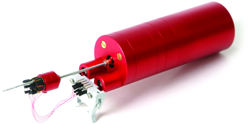
The physical form of a Kelvin Probe is a head unit containing a voice coil driving system and integral amplifier suspended above a sample. The vibrating tip and the sample forms a capacitor, having ideal, or parallel-plate, geometry. As the tip vibrates electric charge is pushed around the external detection circuit. By careful control of the tip potential and automatic capture and analysis of the resulting waveform both the potential across the capacitor and the capacitor spacing can be calculated to very high resolution.
In scanning form the tip is steered across the sample surface using a high resolution 3-axis translator. The spatial resolution of the tip is approximately the tip diameter, we typically use tips of 2.00 mm and 0.05 mm as standard tips in air and anything from a sharp tip to 10.00 mm diameter in ultra-high vacuum. The resulting 3D surface work function images contain information about surface structures, surface composition, thin films, defects, etc. In time-varying mode artefacts such as oxidation (corrosion), defect relaxation, etc can be observed.
For semiconductor surfaces, both organic (polymer) and inorganic (Si, Ge, CdS, etc.) the Kelvin probe is the only way to directly measure the Fermi level. Changes in Fermi level, caused by illumination with white or monochromatic light, results in energy band shifts which can be used to characterise interface and bulk defect states. These techniques are termed Surface Photovoltage (SPV) and Surface Photovoltage Spectroscopy (SPS) for which KP Technology can supply both software and accessories for our systems.
The traditional Kelvin probe actually produces the work function difference between the tip and sample. The Kelvin method was first postulated by the renowned Scottish scientist Lord Kelvin, in 1861. Typically the tip is first calibrated against a reference surface, such as gold. However KP Technology is the only company to offer absolute Kelvin probes, which combine the Kelvin method and Einstein Photoelectric Effect to produce absolute work function values (in eV).
KP Technology has developed dedicated head units for ambient, controlled atmosphere, relative humidity and ultra-high vacuum environments. All of our systems share the off-null, height regulation (ONHR) method invented by Prof. Baikie and consequently produce stable high signal levels resulting in repeatable and high-resolution measurements. The rapid growth of the company since 2000 means the KP Technology systems are found in leading materials research laboratories worldwide. We pride ourselves on our rapid post-sales support and our ability to assist with technical and data interpretation queries.

When a group of atoms or molecules are brought together to form a solid the highest occupied energy level, or Fermi level is termed the work function. The work function is continuous across the interior of the solid, however at the surface the electron energy is influenced by the exact state of the surface, e.g. type orientation and direction of the outer atoms and molecules. Thus different crystallographic orientations of the same solid may have different work functions. The work function of a surface can be modified by adsorbed layers, for instance in corrosion or oxidation of an iron surface, or by modification of composition or controlled contamination as in the case of polymer or inorganic semiconductors.
When two or more materials are brought together the Fermi levels equalise by a flow of electrons from the lower work function to the high. Detecting these electrons this in essence is the way all Kelvin probe systems work.
The work function is often described in introductory textbooks as ‘the energy required to remove an electron from a surface atom to infinity or equivalently the vacuum level’. Although this description appears easy, in surface analysis one has to ask further questions such as which type of electron, where is it taken from and where does it end up?
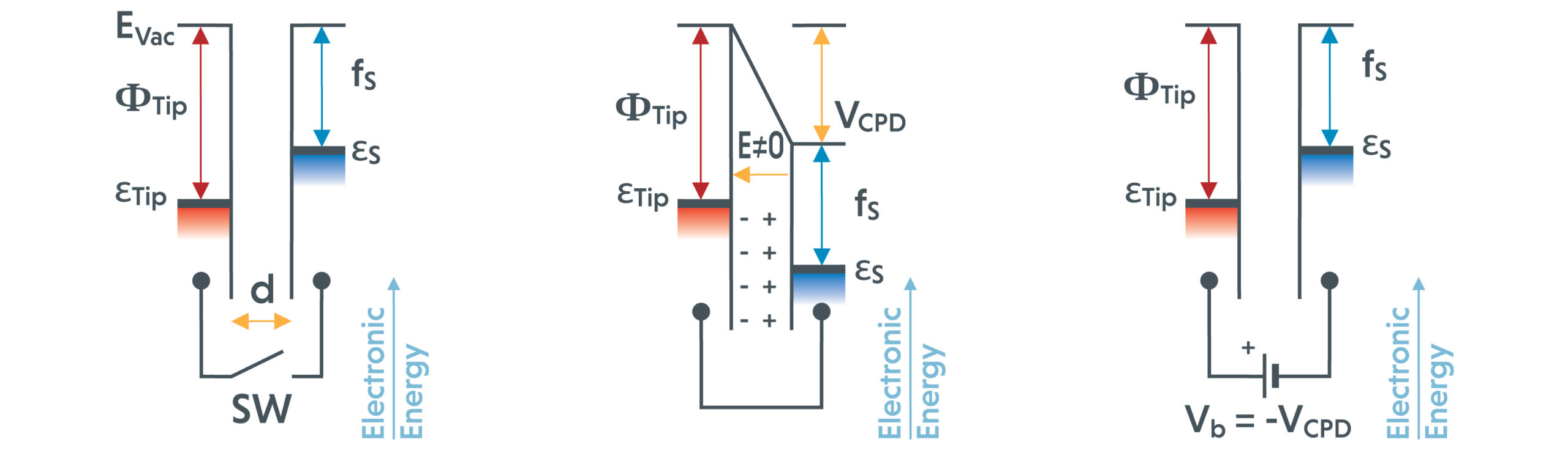
For example as an electron is removed a short distance ‘d’ from a conducting solid there is a so-called attractive image force (due to an imaginary positive charge a distance ‘d’ inside the solid). The force on the electron diminishes as ‘d’ gets larger and by approximately 30 – 50 nm it is exceedingly small. However some work function detection systems actually operate within this region thus the electron is not removed to infinity. This effect, coupled with the local electric fields in the vicinity of the tip, distort the work function data recorded.
In all KP Technology systems the Kelvin probe tip always operates at sufficiently large distances to produce the ‘true work function’ and further the mean spacing of the tip electrode above the sample is tightly controlled producing high-stability, repeatable measurements and allowing automatic system setup.

When light is incident on a material such as a metal or a semiconductor, the photons may have enough energy to liberate electrons from the surface, a process known as the “Photoelectric Effect.”
The energy required for electrons to escape the material is termed the work function. By varying the energy of the incoming light, the absolute work function can be established.
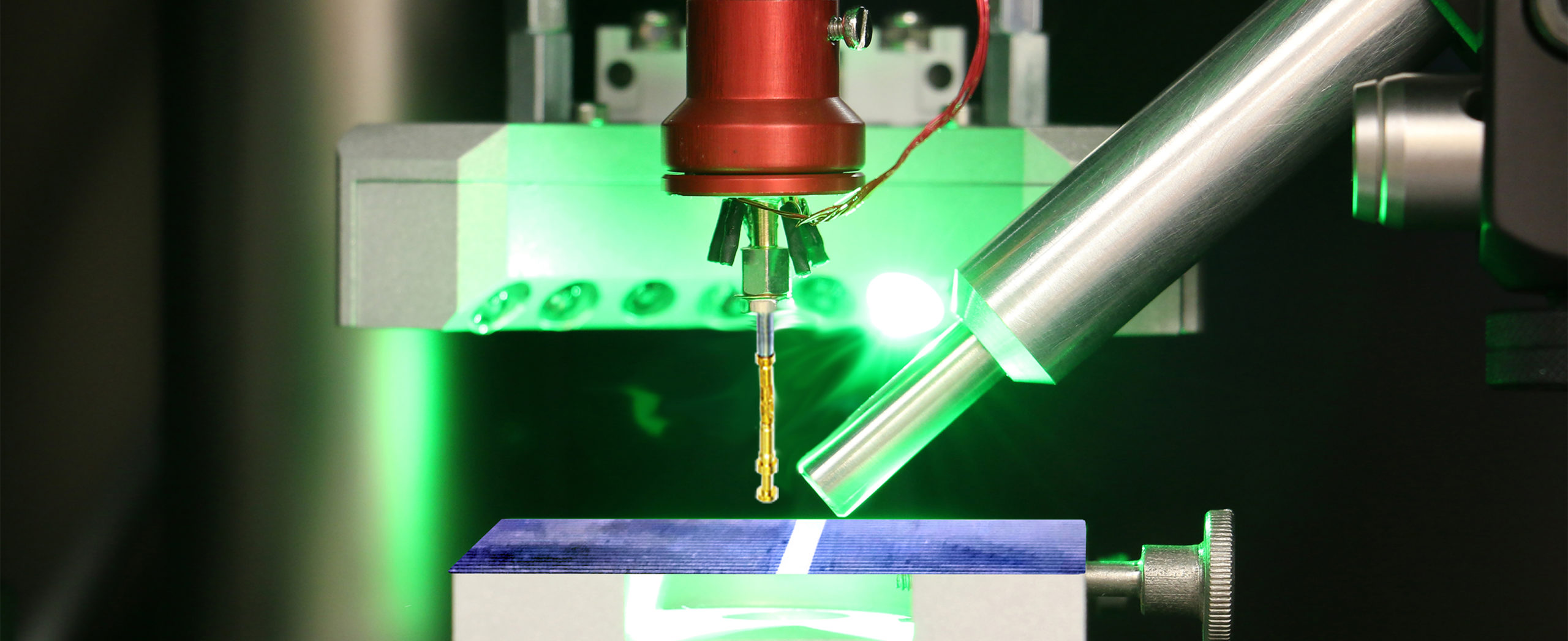
Based on Fowler’s analysis of photoemission, the square root (cube root for semiconductors) of the photoelectron yield is plotted on a graph versus the incident photon energy. The work function of the material under analysis is where this straight line extrapolates to zero.The energy required for electrons to escape the material is termed the work function or volta potential. By varying the energy of the incoming light, the absolute work function can be established.

The properties of many materials are governed by the Density of States (DOS) near the Fermi level. The Ambient Pressure Photoemission Spectroscopy (APS) system is capable of probing the DOS by differentiating the detected photoelectron yield with respect to the incident photon energy. The DOS measurement can thus be compared to molecular orbital calculations for the material under investigation. The data for all samples measured at KP Technology is consistent with literature.

KP Technology systems are based upon unique features developed by Professor Iain Baikie. We are currently in our 7th generation of design, with features unsurpassed by any other company: