The University of St Andrews Organic Semiconductor Centre (OSC) brings together physicists and chemists to undertake collaborative research on remarkable plastic-like materials that can conduct electricity and emit light. Organic materials are an important class of semiconductors as they combine the virtues of plastics, which can be easily shaped, with those of semiconductors which are the basis of all microelectronics. These novel materials can be used to make lightweight flexible optoelectronic devices such as OLEDs, solar cells, lasers, and sensors. Our research extends from fundamental studies of organic molecules and halide perovskites, through device development, to applications in medicine, wireless communications, and explosives detection.
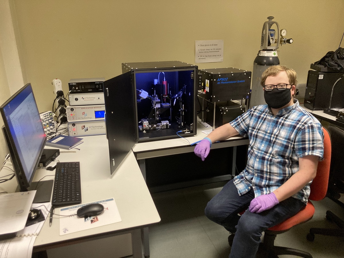
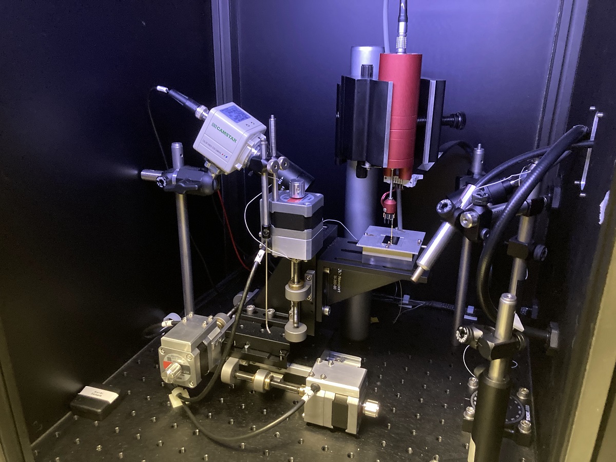
OLEDs, and organic and perovskite solar cells, are normally configured from multiple layers of materials, selected to transport charges, or control the recombination or dissociation of excited states. It is therefore crucial for the optimisation of these devices to have a complete understanding of the energy levels of the materials, and how they align when layered in a device. We use both ambient pressure photoelectron spectroscopy, and Kelvin probe measurements to characterise these energy levels. Our APS03 system from Kelvin Probe Technology has therefore been an essential tool in the development of both high efficiency photovoltaics for indoor energy harvesting, and high brightness and very fast OLEDs used for medical lighting and for wireless communications.
We have worked directly with KP Technology through two PhD projects, exploring new applications of the equipment. These students have studied a diverse range of systems, including halide perovskites, organic semiconductors, synthetic diamond, and fingerprint detection.
The School of Physics and Astronomy also uses a Scanning Kelvin probe in the senior teaching laboratory. We have integrated this into our teaching programmes for both undergraduates and postgraduates. The Kelvin probe is a popular experiment that enables students to explore concepts of work functions of metals, Fermi levels and doping in semiconductors. Using surface photovoltage measurements, students gain insight to charge trapping in semiconductors and to the built-in voltage in a p-n junction. The Kelvin Probe Technology equipment has been an excellent asset in students’ learning of sustainable power generation technologies and quantum properties of materials.